Via filling
Customer requirement: "Vias covered"
Customer requirements
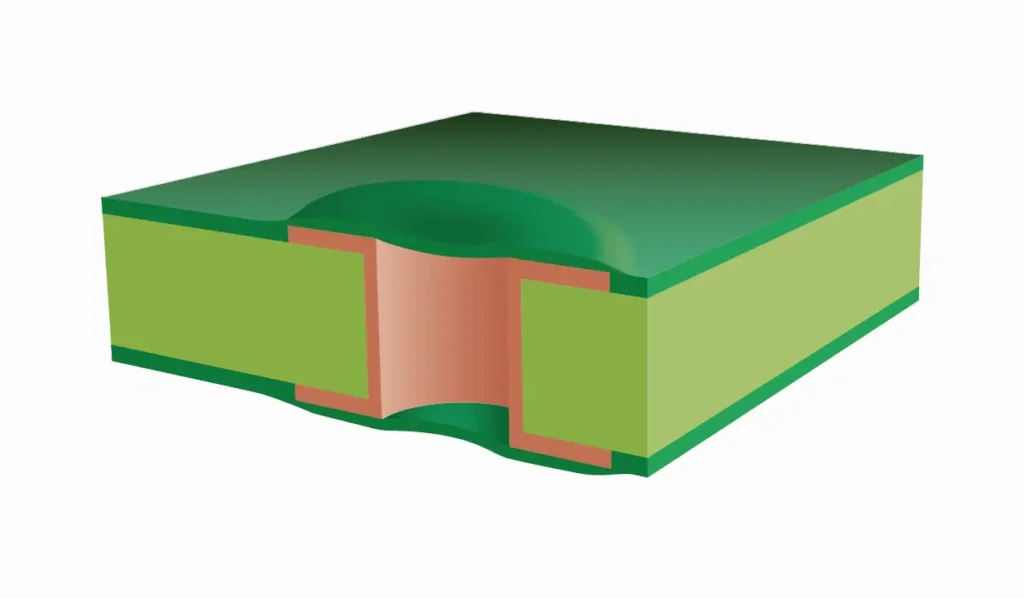
Cover the vias with solder resist in one step to completely cover the hole and prevent solder from flowing through.
Usually with dry film technology. Dry film solder resist is no longer common and rarely available on the market.
Wishful thinking
Even flow of paint into the hole from one or both sides.
These specifications do not meet the relevant quality requirements and are therefore NOT recommended! Recommendation: see right!
Ideal case

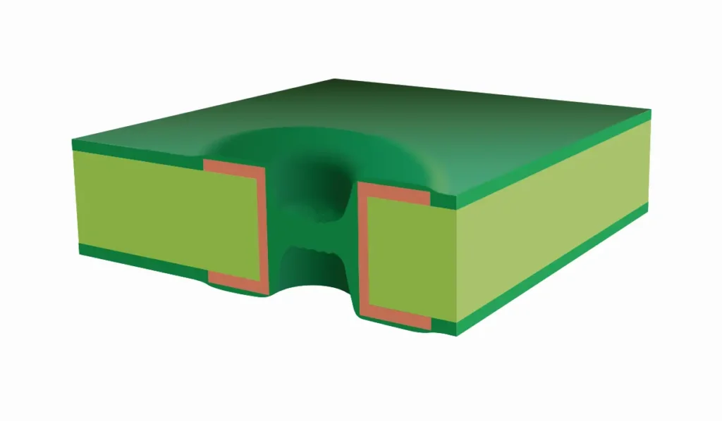
Uncontrolled filling of the hole but complete covering of the hole wall.
Reality
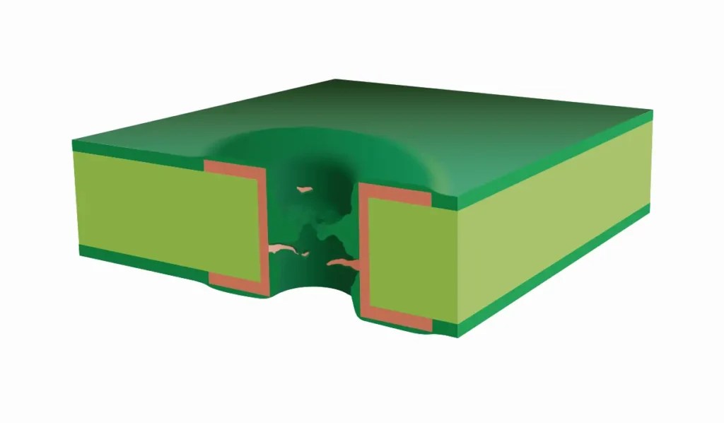
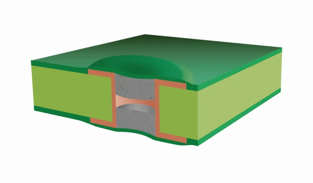
Incomplete covering of the inner hole wall of the via. Danger of chemical
inclusions or residues and ionic contamination. There is a risk of blow-outs or soldering problems.
Quality problems are to be expected.
No guarantee of manufacturer.
Covering the vias in Asian production facilities
Vias are usually covered with solder resist using screen printing according to the Gerber data. Below 0.4 mm, the result is usually acceptable (with the risk of inclusions). Above 0.4mm the risk of inclusions increases and soldering problems can occur. There is no guarantee or assumption of consequential damages.
Via-Filling vs. Via-Plugging
The IPC-4761 defines the difference between filling and plugging. Plugging is not recommended, as considerable
disadvantages exist.
Recommendation: Via-Filling!
Via filling
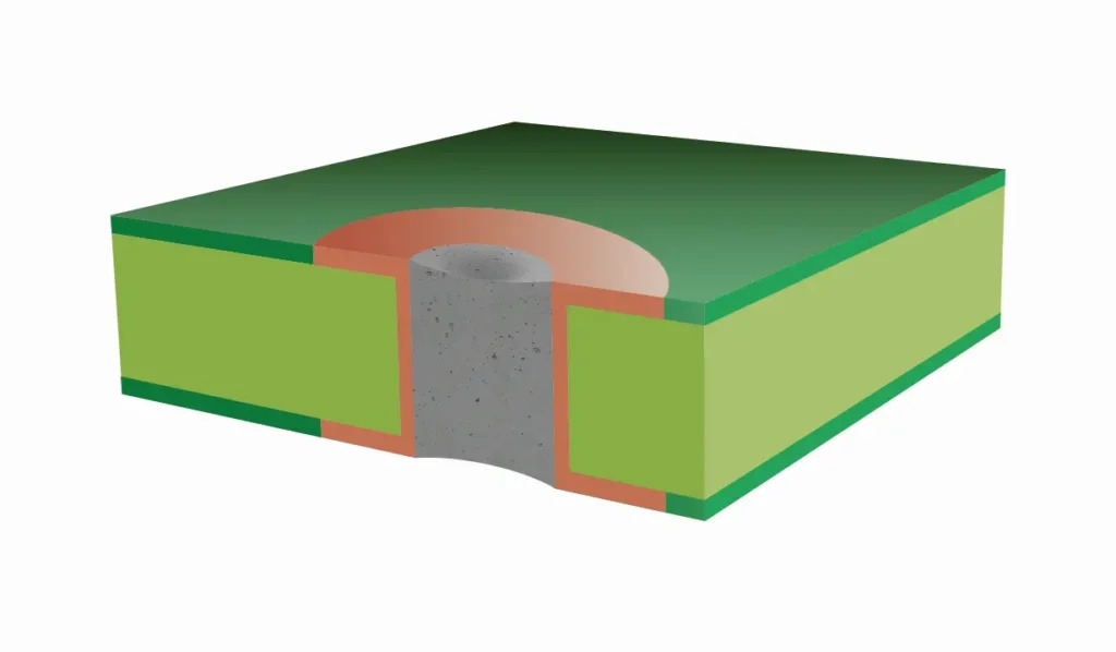
Via-Plugging
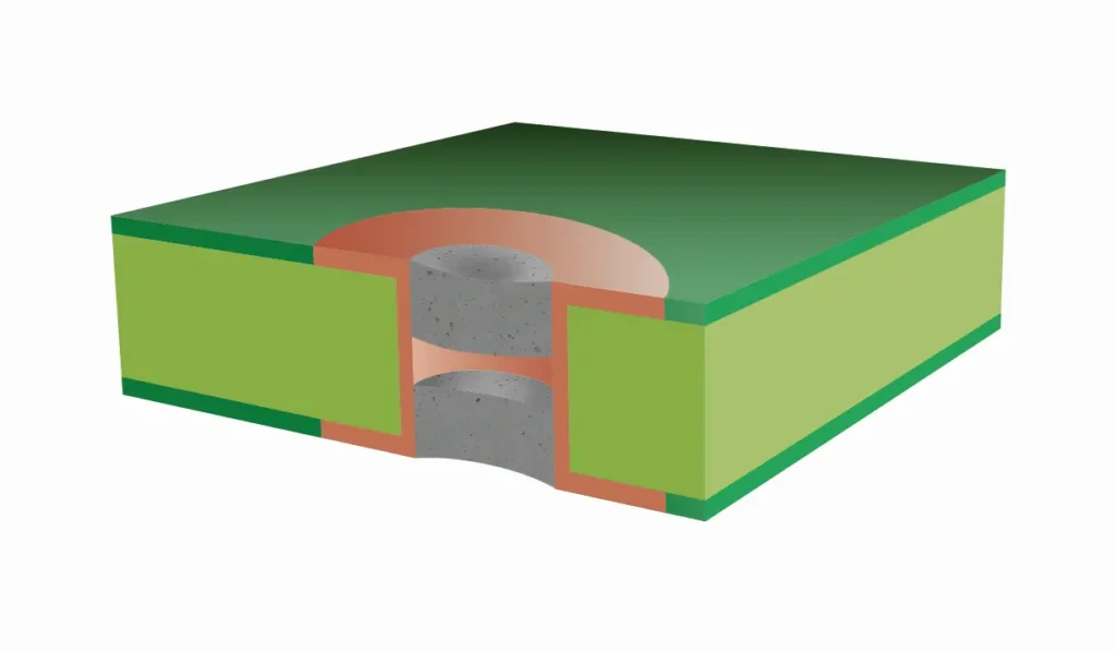
Recommended versions of the vias
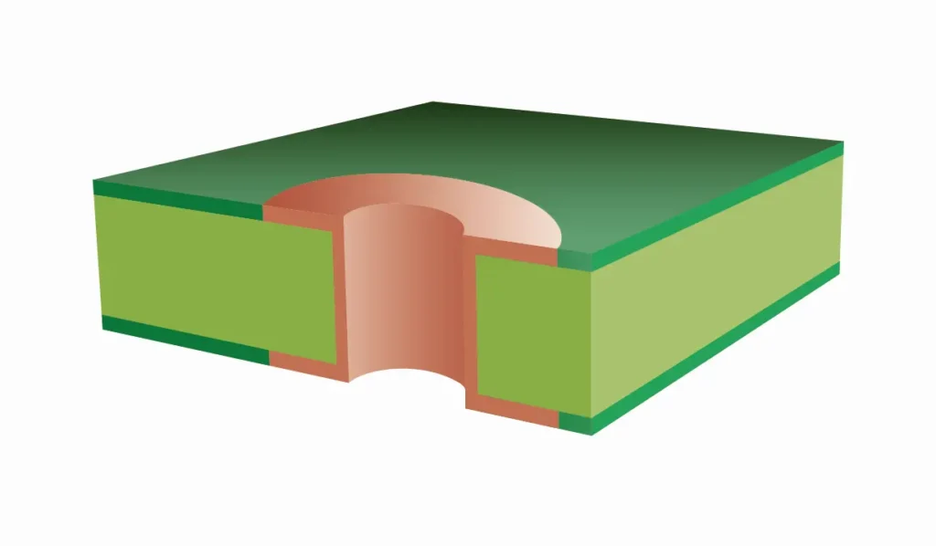
Open Vias (Via Type 0)
Standard process. Viapad complete exposed from solder resist.
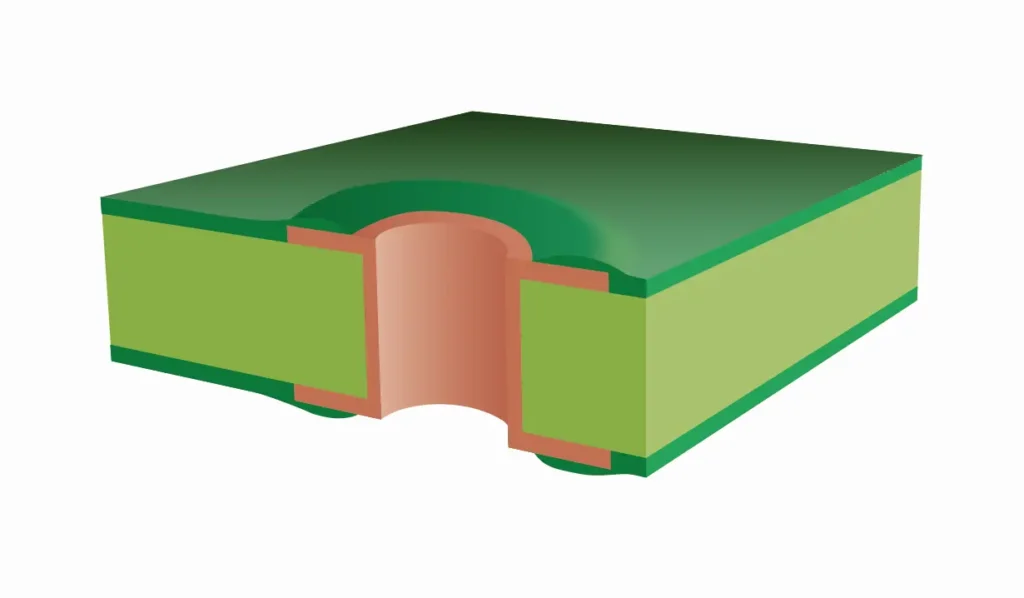
Pad covered, hole exposed (via type 0a)
Most of the Viapad is covered with solder resist. Only the hole with a minimal residual ring remains open on both sides.
Notes on type 0 and type 0a
The minimum hole size for spray paint is 0.3 mm (drilled 0.4 mm) and for screen printing 0.5 mm (drilled 0.6 mm) in order to achieve perfect cleaning of the paint ink in the hole.
The volume of residue in the holes also depends on the color of the solder mask, the copper thickness and the PCBauch: gedruckte Schaltung, engl.: PCB – Printed circuit boar… More thickness
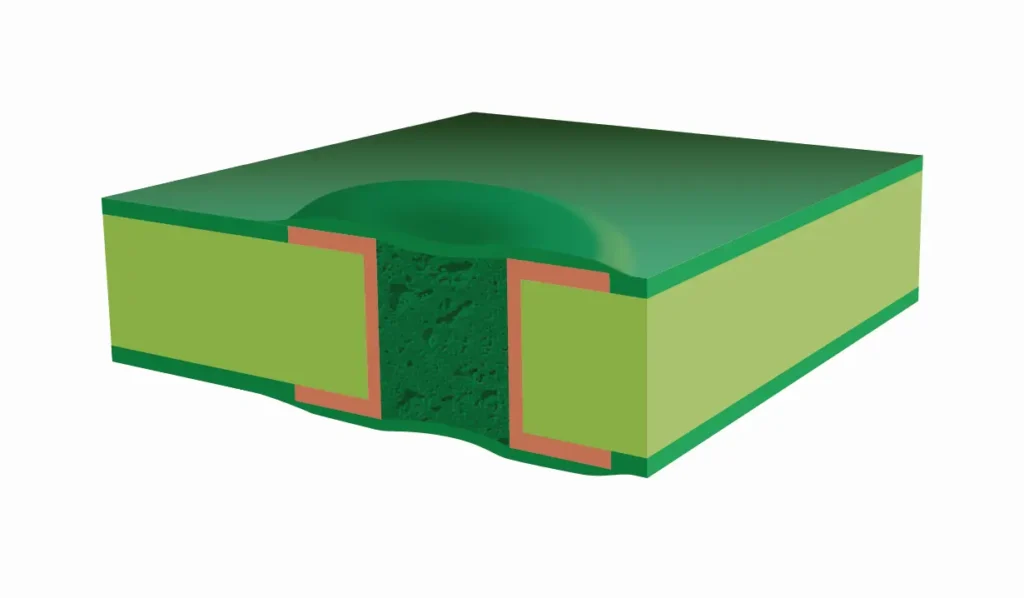
Via filling with solder resist (Via type 0b)
The hole is filled with a solder resist recommended by the paint manufacturer and cured in a separate process. In the normal solder resist process, the pad can now be coated with
solder resist and offers optimized reliability.
This process does not comply with the IPC recommendations. Complete filling cannot be guaranteed.

Via filling with resin (via type V)
Resin-filled vias. Airtight packed vias, recommended by the IPC.
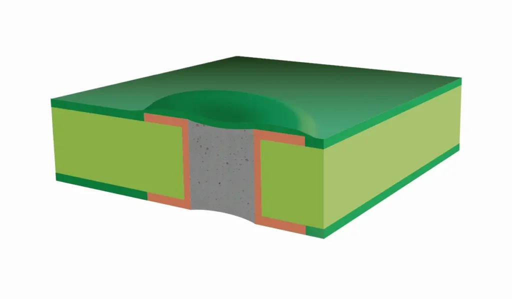
Via type VIa
Resin-filled via like type V, but covered on one side with solder resist on the top or bottom.

Via type VIb
Resin-filled via like type V, but covered with solder resist on both sides.
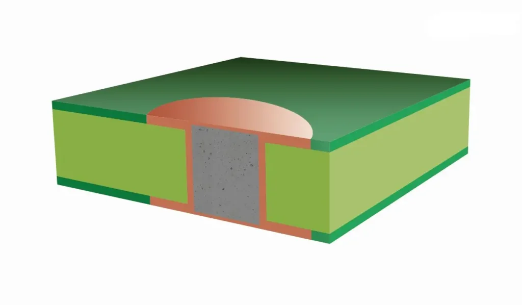
Via-Filling & Capping (Via Type VII)
Via-filling with resin and copper capping. Ideal for via-in-pad technology. Can be assembled and soldered.
| Via filling with ... | Resin | Solder resist |
|---|---|---|
| Hole size (final) min-max | 0,1mm-0,7mm | 0,1mm-0,5mm |
| Material thickness | 1,00-2,40mm | 0,50mm-3,20mm |
| UL certified | Yes (depending on material) | Yes |
| Via-In-Pad | Yes | No |
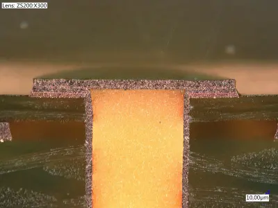
IPC viatypes I to IV (Use not recommended!)
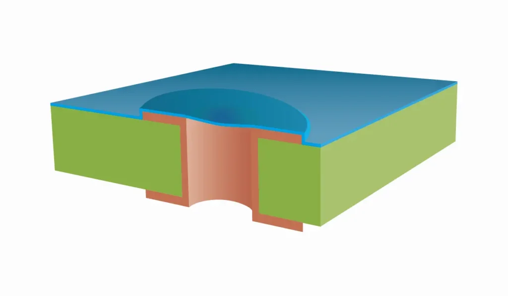
Via Type Ia
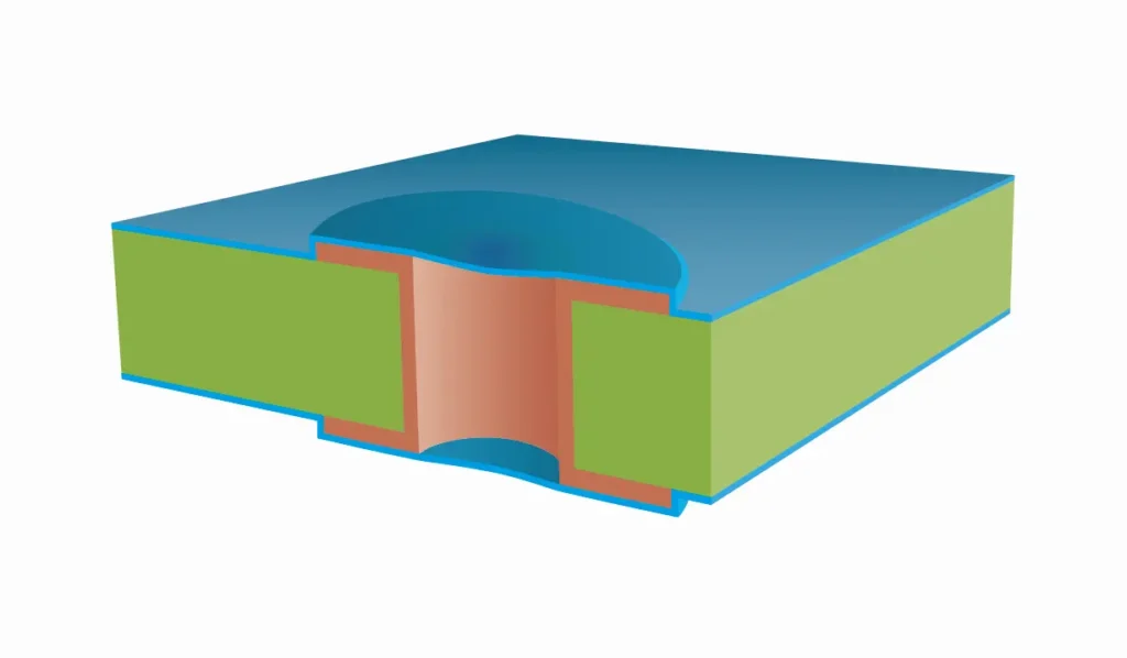
Via Type Ib
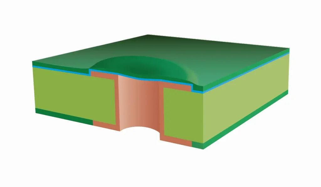
Via Type IIa
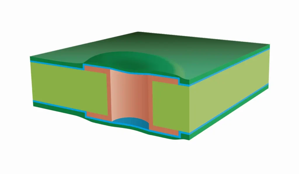
Via Type IIb
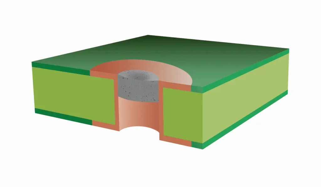
Via Type IIIa

Via Type IIIb
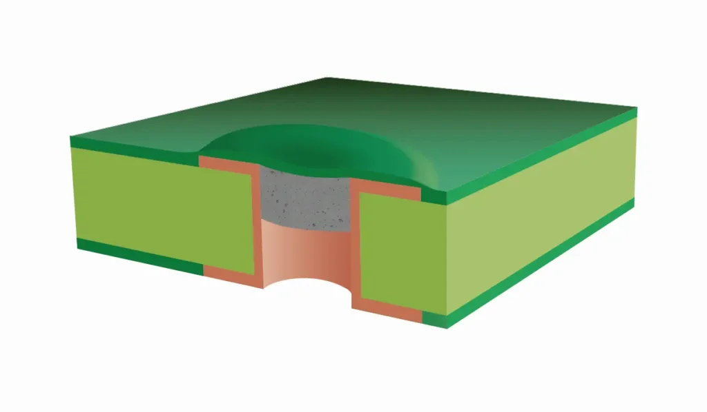
Via Type IVa
