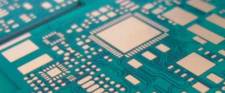
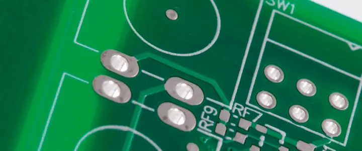
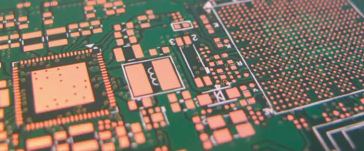
The surface treatment increases the wettability of the solder connection surfaces during the soldering processes. Non-chemical surfaces also act as protection against oxidation of the underlying copper surfaces and increase the storage life.
The surface treatment of PCBs is an important aspect in electronics production, as it influences the electrical conductivity, solderability and corrosion resistance of the printed circuit boardauch: gedruckte Schaltung, engl.: PCB – Printed circuit boar… More. Here are some of the most common surface treatments for printed circuit boards from a technical point of view:
| Surface | Advantages | Disadvantages |
|---|---|---|
|
Hot-Air-Levelling - HAL
also: HASL - Hot-Air-Solder-Levelling The flux-wetted circuit board is dipped into liquid tin and blown off with hot compressed air when it is pulled out. |
Good solderability Shelf life Optimized reflow |
Pads not flat Tin drops Thermal stress |
|
Chemical Tin (Immersion Tin, Electroless Tin)
The properties of this chemically applied surface are very similar to those of HAL. A thin layer of tin is applied chemically to ensure a very flat surface. |
Flat pads
SMD optimized Suitable for fine pitch |
Rapid oxidation
Strict handling Limited shelf life Surcharge Susceptible to tin-whisker formation |
|
Chemical Silver (Immersion Silver) is a chemically applied, absolutely flat surface, similar to chemical tin. The properties in terms of oxidation and processing are superior to those of chemical tin. |
Plane pads
SMD optimized good shelf life |
Surcharge |
|
Chemichal Gold - Chem. Ni/Au (Electroless Nickel Immersion Gold) - ENIG
The extremely flat surface and very good oxidation properties can be easily processed by all assemblers. In this process, a nickel layer is applied in a chemical process first. This prevents the copper from diffusing into the chemically applied gold layer. |
Plane Pads
SMD optimized Very good wetting, shelf life Optimal temperature resistance |
Surcharge Not recommended for some HF PCBs |
|
Electroless nickel Palladium Gold (ENEPIG)
is similar to chemical gold and also has a separating layer of palladium between the nickel and gold layers. It is ideal for bonding aluminum and gold wires. |
Plane pads
SMD optimized Optim. Wetting Shelf life Suitable for bonding |
Surcharge Not recommended for some HF PCBs |
|
OSP - (Organic Solderability Preservative)
is a vapor-deposited soldering lacquer on an organic basis. Multiple soldering must be carried out in a nitrogen atmosphere due to the temperature sensitivity. It provides a temporary protective layer against corrosion and enables good solderability. OSP surfaces are sensitive to environmental conditions and should not be stored for long periods of time. |
Favorable price |
Restricted
storable
Limited multiple soldering Strict handling |
|
Galvanic gold (electroplated) Soft gold for gold wire bonding, hard gold for gold plugs and sliding contacts A galvanically applied surface with a nickel base, for hard gold plugs, for example (see also chapter "edge connector"), selective gold surfaces or bonding pads. |
For special applications |
High surcharge
Danger of a reaction with other surface finishes. |
Choosing the right surface treatment depends on the specific requirements of your PCBauch: gedruckte Schaltung, engl.: PCB – Printed circuit boar… More application, including soldering processes, environmental conditions and costs. The right surface treatment can have a significant impact on the service life and performance of your PCBauch: gedruckte Schaltung, engl.: PCB – Printed circuit boar… More.
| Surface | RoHS | Solderable |
Bond AL-wire |
Bond Au-wire |
BGA µBGA |
Flex Rigidflex |
Pressfit technology |
surface contacts |
Layer thickness |
Shelf life* |
solder cycles |
|
|---|---|---|---|---|---|---|---|---|---|---|---|---|
| Tin | HASL SnPb | NO | YES | - | - | - | - | YES | - | 5-40µm | 6 months | multiple |
| HASL | YES | YES | - | - | - | - | YES | - | 5-40µm | 6 months | multiple | |
| ISn | YES | YES | - | - | - | - | YES | - | >1µm | 3 months | 2 | |
| Silver | IAg | YES | YES | YES | - | - | YES | YES | - | >0,2µm | 6 months | multiple |
| Gold | ENIG | YES | YES | YES | - | YES | YES | YES | - |
3-5µm Ni >0,04µm Au |
6 months | multiple |
| ENEPIG | YES | YES | YES | YES | YES | YES | YES | - |
4-7μm Ni 0,2 μm Pd >0,01 μm Au |
6 months | multiple | |
| GAu Soft | YES | YES | - | YES | - | - | - | - |
3-5μm Ni 0,05 μm Au |
12 months | - | |
| GAu Hard | YES | - | - | - | - | - | - | YES |
3-5μm Ni upto 1 μm Au |
12 months | - | |
| Solder varnish | OSP | YES | YES | - | - | YES | - | YES | - | 0,3-0,5 μm | 6 months | ** |
GAu = Galvanic (electrolytic) Gold
*Storage time recommendations based on the IPC storage conditions
Longer storage times are possible in individual cases, depending on a wetting test
**Multiple soldering possible, with optimal production planning
All specifications are to be understood as guidelines of the respective process manufacturers and may deviate in individual cases.
Please also refer to the page “storage“.

