Peelable Mask
Peelable mask is used to cover areas where solder is prevented from penetrating metallized holes or tinning solder pads during wave soldering. Furthermore, a peelable mask can be used in the area of gold contacts or carbon elements. The peelable mask can withstand the PCBauch: gedruckte Schaltung, engl.: PCB – Printed circuit boar… More being heated twice without peeling off.
After the soldering process, the mask can be removed from solder pads and plated-through holes without leaving any residue.
Caution: No peelable mask should be applied to non-plated-through holes, slots or contours, as residue-free removal cannot be guaranteed.

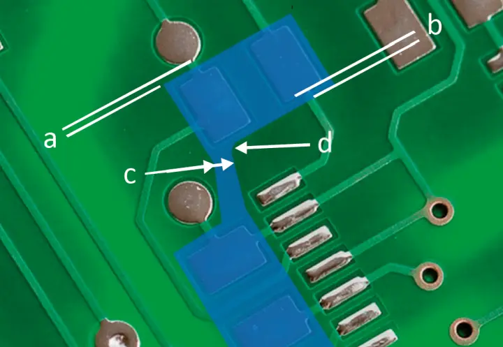
| Property | Standard | |
|---|---|---|
|
|
a | ≥0,5mm |
| Overlap Peelable mask | b | ≥0,5mm |
| Min. bridge wdth | c |
≥1,5mm Recommendation: ≥2mm |
| Internal angle/corners | d |
≥90° Recommendation: Rounded |
These recommendations do not represent the technological limits.
Please discuss this with the manufacturer.
To avoid excessive paint flow and paint leakage on the opposite side, drill holes with a diameter of > >1.0 mm should not be completely covered by strippable paint. Complete coverage (closure) cannot be guaranteed for holes > >2.0mm. We recommend covering these holes with capton tape.
Carbon print
Carbon pastes are fine or coarse-grained graphite pastes that are applied by screen printing as keyboard contacts, LCD contacts or LCD strips. There are basically two types:
- Resistive graphite printing for sliding contacts
- Conductive graphite printing for membrane contacts
Due to the requirements for carbon print, a minimum copper thickness of 17.5μm is required. A peelable mask (see above) can also be applied to protect the carbon layer.


In the Gerber data, the data for the carbon print (here: gray) should be output as a separate file.
List of data
- Contour (light gray)
- Copper (red)
- Legendprint (white)
- Carbon print (grey)


