Electrical testing
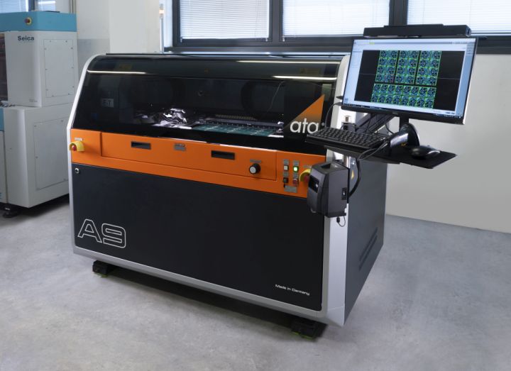
For quality assurance purposes, all multilayers and bilayers from small series onwards (also possible for single-sided PCBs on request) are subjected to 100% electrical testing. The check is carried out using a netlist generated from the CAD data. For
sample deliveries are tested using flying probes (finger testers); for series production, testing using needle adapters (parallel test) is more economical.

Picture: Flying Probe-Tester ATG A9
AOI test
After the etching process, the inner layers of a multilayerMultilayer (Mehrschicht-Technologie):Die Multilayer-Technolo… More are subjected to an AOIAutomated Optical Inspection AOI ist ein Begriff in der Elek… More (Automatic Optical Inspection). Special double-sided PCBs, for example with attached coils, are also subjected to an AOIAutomated Optical Inspection AOI ist ein Begriff in der Elek… More. The etched conductor pattern is scanned in high resolution and automatically compared with the CAD data specifications. Detection of short circuits, interruptions, constrictions, foreign particles, distance underruns, etching faults, etc. Detected faults are verified manually and sent for appropriate fault handling.
Other test methods
A large number of other test procedures are available in the
productions.
- Impedance control / coupon test
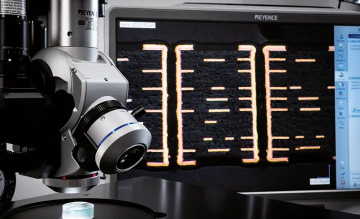
- Microsection incl. metallurgical analysis
- Coating thickness determination
- Climate test
- Shock and stress test
- Mechanical testing with precision instruments
- Micrometric depth control for scoring lines
- Process control for structural thicknesses
- Optical 3D inspections
- X-ray test for drill centering
- Ion contamination tests
Detailed test reports or an initial sample test report are enclosed with the delivery of your printed circuit boards.

Picture: Keyence Mikroskop


