In this guide, we would like to provide you with suggestions and information for all questions relating to the design of your perfect stencil, the optimum layout design, the optimum pad image and the selection of the right stencil thickness. Our experts will be happy to provide you with advice and assistance.
The quality of the laser-cut stencil is crucial for a stable production process in solder paste printing. The volume, size and uniformity of the solder deposits are determined by optimally adapting the pad design, choosing the right material thickness and optimum production parameters.
Basic design rules such as the area ratio (printed area in relation to the pad inner wall area) and the aspect ratioAspect Ratio (Seitenverhältnis)Das Aspect Ratio oder Seiten… (ratio of pad width in relation to stencil thickness) must be observed. The IPC – Association Connecting Electronics Industries® has published the basic requirements for SMT design and SMD connection surfaces in its IPC-7351B guideline.
Goals
- Perfect print results
- Precisely adjusted lot quantity for each depot
- Prevention of bridging
especially between small solder deposits - Avoidance of tearing off the solder paste during
Lifting the stencil - Prevention of solder balls
- Avoidance of tombstone effects
- Improvement of the printing process through
Optimized unrolling of the solder paste


Laser cutting
- Precision sheet metal with optimum properties
- Edge roughness 3-4μm
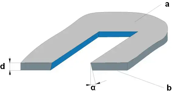
- Pads conically cut, bevel of the edges approx. 5°
- Laser entry side = burr-free LP side slightly wider due to the bevel
- Laser exit side = squeegee side
The result of the optimally designed laser cutting is a significantly improved release behavior of the solder paste compared to vertical pad inner edges.
Correct choice of material
- The smallest component is always decisive
- Rule of thumb: pad width/1-1.5 = stencil thickness
- Common based on the average components and layout: 120-150μm, 180μm
- For BGA, μBGA, FinePitch, High-Density: 80μm, 100μm, 120μm, 130μm
Calculation
Aspect RatioAspect Ratio (Seitenverhältnis)Das Aspect Ratio oder Seiten…
b / d > 1,7
Area Ratio
(l x b) / 2x (l + b) x d > 0,8
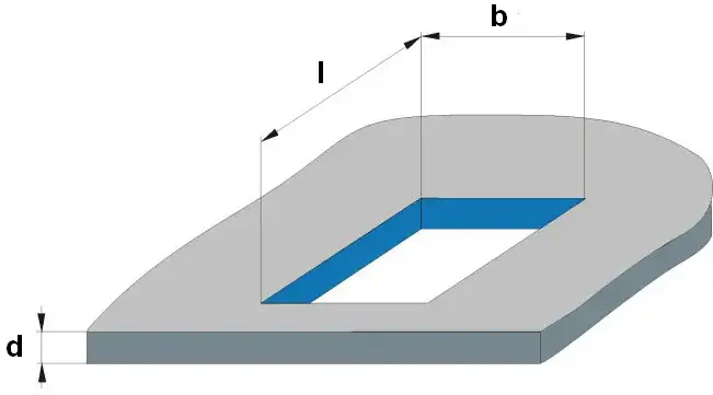
b= Pad width, l = Pad length
d = Stencil thickness
Recommended stencil thicknesses
Component shapes determine the adaptation of the pad geometry and the stencil thickness. In the following table, we would like to provide you with guide values that have proven to be good empirical values based on many projects. These are approximate values! The final decision should always be made after viewing the complete layout.
| Design/component | Pitch mm | Padwidth µm | Recomm. thickness µm |
|---|---|---|---|
| BGA | 1,25 | 630 | 150-180 |
| 0,8 | 420 | 150 | |
| Finepitch BGA | 1,00 | 500 | 150 |
| µBGA | 0,5 | 75-120 | |
| IC | 0,5 | 240 | 150 |
| 0,65 | 320 | 150 | |
| 0,8 | 380 | 180 | |
| >0,8 | 25-30* | 200 | |
| 01005 | 0,4/0,2 | 20-30* | 120 |
| 0201 | 0,6/0,3 | 20-30* | 150-180 |
| 0402 | 1,0/0,5 | 20-30* | 180 |
| SCP | 0,65 | 320 | 120 |
| PLCC | 1,25 | 150-250 | |
| QFP | 0,65 | 150-180 | |
| 0,5 | 125-150 | ||
| 0,4 | 100-130 | ||
| 0,3 | 75-130 |
*Circumferential reduction in μm
Data processing
The quality of the laser-cut stencil is crucial for a stable production process in solder paste printing. The volume, size and uniformity of the solder deposits are determined by optimally adapting the pad design, choosing the right material thickness and optimum production parameters. Basic design rules such as the area ratio (printed area in relation to the pad inner wall area) and the aspect ratioAspect Ratio (Seitenverhältnis)Das Aspect Ratio oder Seiten… (ratio of pad width in relation to stencil thickness) must be observed. The IPC has published the basic requirements for SMT design and SMD connection surfaces in its IPC-7351B guideline.
Usual design adjustments
- General reduction of all pads by 10%
- Circumferential equal reduction of pads (e.g. 20-50μm smaller)
- Overprinting: enlargements to achieve the required depot quantity
- Individual components are treated individually
- 50:50 rule: pad width should not be greater than bridge width
