The generally accepted specifications for copper thicknesses on printed circuit boards such as
18µm (hoz), 35µm (1oz) or 70µm (2oz),
etc. are in clear contradiction to the technical conditions.
How are the details to be understood?
Basic information
The ounce rating has its roots in the gold foil industry and subsequently for the use of copper in the construction industry. It is based on the distribution of one ounce of a particular metal over one square foot of surface area.
Since the topography of the treated sheet varies greatly and the density of the copper is known, weighing a 1 x 1 foot sheet is the best way to determine the average thickness of a copper sheet; thus, the volumetric weight in ounces/ ft² (oz/ft² or just oz) is the usual unit of measurement.
In Europe, on the other hand, the copper specification is given in metric and defined as “thickness in µm”, which results in a corresponding conversion.

Cause of problem
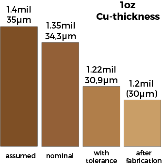
1 ounce of copper per square foot is nominally 0.00135 inches or 34.3 µm thick, as shown in the summary table.
The specification 35µm has become established. The incorrect rounding to the µm nominal values results in the following incorrect values: 0.7mil (18µm), 1.4mil (35µm), 2.8mil (70µm).
Unfortunately, these specifications are still predefined in many EDA tools. In the case of a high layer multilayerMultilayer (Mehrschicht-Technologie):Die Multilayer-Technolo… More with 16 or more layers, for example, this difference may also have a significant effect on the PCBauch: gedruckte Schaltung, engl.: PCB – Printed circuit boar… More thickness.
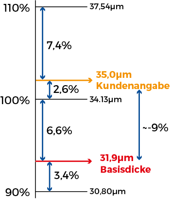
According to the IPC, the minimum thickness of the film must not be more than 10% below the nominal value, which the film manufacturers naturally put into practice and thus save money.
The picture:
According to the material manufacturer’s data sheet, the average values are 280-285g/m², which corresponds to a shortfall of around 7% from the nominal value. The base thickness therefore defines the real starting value of the copper layer of the base material!

Copper weight conversion
|
Copper weight oz/ft² |
Conversion g/m² |
Nominal thickness (nominal) |
after production |
90% of the Nominal thickness |
|---|---|---|---|---|
| 1/4 oz | 75,9 g/m² | 0,34mil (8,5μm) | 0,3mil (7,5μm) | 0,31mil (7,65μm) |
| 1/2 oz | 152 g/m² | 0,68mil (17,1μm) | 0,6mil (15μm) | 0,61mil (15,4μm) |
| 1 oz | 305 g/m² | 1,35mil (34,3μm) | 1,2mil (30μm) | 1,22mil (30,9μm) |
| 2 oz | 610 g/m² | 2,70mil (68,6μm) | 2,4mil (61μm) | 2,43mil (61,7μm) |
Process reduction
The thickness of copper foils is reduced several times during LP production by chemical or mechanical processes. The IPC specifies a max. permissible process reduction for outer and inner layers as follows:
| Outer layers | Inner layers | |||||
|---|---|---|---|---|---|---|
|
Copper weight oz (µm) |
Absolute Cu minimum |
Process reduction |
Final according to IPC Class 2 |
Final according to IPC-Class 3 |
Process reduction |
Final according to Inner layer prod. |
| 1/4oz (8,6μm) | 0,30mil (7,7μm) | 1,50μm | 26,20μm | 31,20μm | 1,50μm | 6,20μm |
| 1/2oz (17,10μm) | 0,61mil (15,4μm) | 2,00μm | 33,40μm | 38,40μm | 4,00μm | 11,40μm |
| 1oz (34,30μm) | 1,22mil (30,9μm) | 3,00μm | 47,90μm | 52,90μm | 6,00μm | 24,90μm |
| 2oz (68,60μm) | 2,43mil (61,7μm) | 3,00μm | 78,70μm | 83,70μm | 6,00μm | 55,70μm |
The usual values for copper plating as an addition to the base copper for IPC class 2 are min. 20µm and for IPC Class 3 at min. 25µm.
Conversion table
| Conversions | |
|---|---|
| 1 oz (ounce) | = 28,35 g |
| 1 ft | = 30,48 cm |
| 1 ft² | = 0,093 m² = 930 cm² |
| Specific Cu weight | = 8,9 g/cm³ |
Cost information
“Incorrect” information often leads to misunderstandings in the calculation. Specifications according to the motto “more is better”, without considering the price effect, often cause prices to be too high. The technological effect on the etching result if the structures are too fine should also not be ignored.
The average price increase at 70μm is around 15-20%, at 105μm even around 30%. It is therefore important to check at the inquiry stage whether approx. 50μm final copper after production (with 35μm base copper) is actually sufficient and the price of the PCBauch: gedruckte Schaltung, engl.: PCB – Printed circuit boar… More can be reduced.
Recommended spacing depending on copper thickness
| Cu base foil | 18 µm | 35 µm | 70 µm | 105 µm | 140 µm | 175 µm | 210 µm | 300 µm |
|---|---|---|---|---|---|---|---|---|
| Track width |
0,1 mm 4 mil |
0,15 mm 6 mil |
0,2 mm 8 mil |
0,3 mm 12 mil |
0,4 mm 16 mil |
0,5 mm 20 mil |
0,7 mm 28 mil |
1,0 mm 24 mil |
| Restring** |
0,15/0,10 6/4 mil* |
0,2/0,15 8/6 mil* |
0,2 mm 8 mil |
0,3 mm 12 mil |
0,4 mm 16 mil |
0,5 mm 20 mil |
0,7 mm 28 mil |
1,0 mm 24 mil |
| Distances |
0,1 mm 4 mil |
0,15 mm 6 mil |
0,2 mm 8 mil |
0,3 mm 12 mil |
0,4 mm 16 mil |
0,5 mm 20 mil |
0,7 mm 28 mil |
1,0 mm 24 mil |
| Drill-Ø |
0,2 mm 8 mil |
0,3 mm 12 mil |
0,3 mm 12 mil |
0,35 mm 14 mil |
0,4 mm 16 mil |
0,5 mm 20 mil |
0,5 mm 20 mil |
0,6 mm 24 mil |
Note:
Recommendations do not represent the technological limits. Please discuss this with the respective manufacturer.
* Inner-/Outerlayers
** Restring means the circumferential ring of the copper pad in a drilled hole.
Calculation: (pad diameter – final drilling diameter)/2


