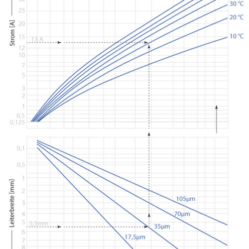
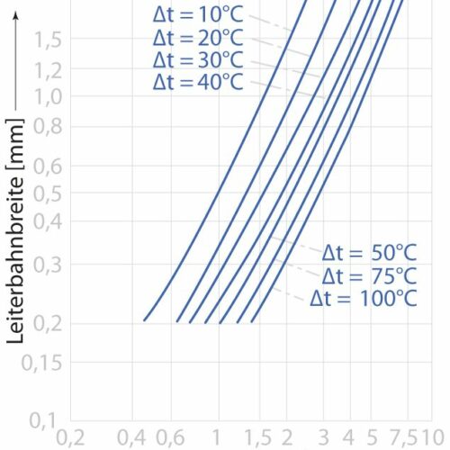
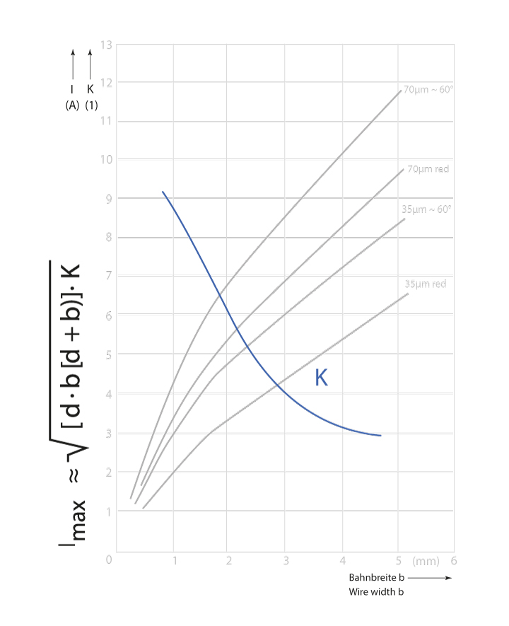
Ampacity, conductor cross-section and temperature are decisive factors in the design of printed circuit boards, especially in electronic applications. Correct dimensioning and consideration of these parameters play a key role in the performance and reliability of printed circuit boards.
In this context, the following charts and diagrams provide valuable insights and findings that illustrate the importance of these factors. These visual aids make it possible to better understand the interactions between current carrying capacity, trace cross-section and temperature and help to develop optimized PCBauch: gedruckte Schaltung, engl.: PCB – Printed circuit boar… More layouts that meet the requirements of electronic circuits in terms of performance and reliability. In the following sections, we will explain these key aspects in more detail and use the information from the accompanying charts and diagrams to deepen our understanding.
Conductor cross-section, temperature
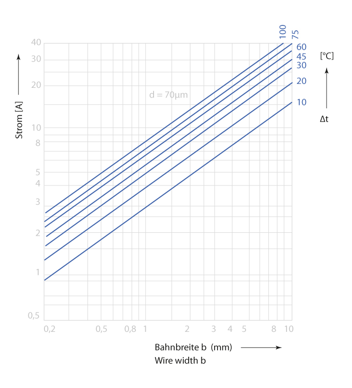
Ampacity
Temperature coefficients
for copper thicknesses 35µm and 70µm
35µm
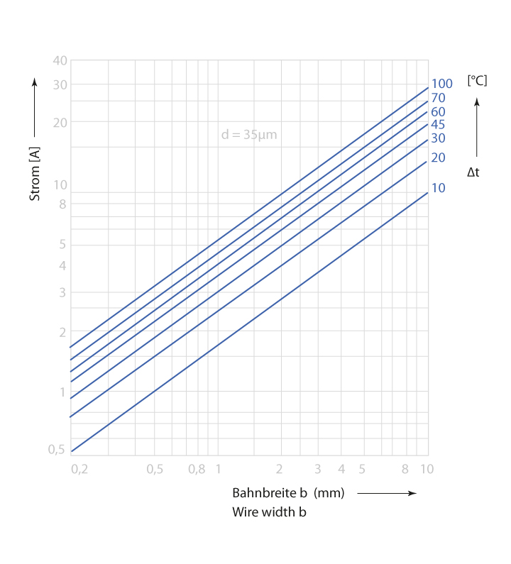
70µm
Insulation distances
Minimum electrical distances for internal distances “conductor track to conductor track” and “conductor track to plated-through hole” depending on sea level are shown in the following table.
The voltage values apply to DC voltage or peak/peak for AC voltage. With AC voltage, the frequency can lead to a reduction in the dielectric strength of materials, so various design parameters should be taken into account.
| PCB | Electronic device | |||||
|---|---|---|---|---|---|---|
| Voltage | L1 | L2 | L3 | L4 | FB1 | FB2 |
| 0-15V | 0,10mm | 0,64mm | 0,64mm | 0,13mm | 0,13mm | 0,13mm |
| 16-30V | 0,10 mm | 0,64mm | 0,64mm | 0,13mm | 0,25mm | 0,13mm |
| 31-50V | 0,10mm | 0,64mm | 0,64mm | 0,13mm | 0,38mm | 0,13mm |
| 51-100V | 0,10mm | 0,64mm | 1,50mm | 0,13mm | 0,50mm | 0,13mm |
| 101-150V | 0,20mm | 0,64mm | 3,18mm | 0,38mm | 0,75mm | 0,38mm |
| 151-170V | 0,20mm | 1,27mm | 3,18mm | 0,38mm | 0,75mm | 0,38mm |
| 171-250V | 0,20mm | 1,27mm | 6,40mm | 0,38mm | 0,75mm | 0,38mm |
| 251-300V | 0,20mm | 1,27mm | 12,70mm | 0,38mm | 0,75mm | 0,38mm |
| 301-500V | 0,25mm | 2,54mm | 12,70mm | 0,75mm | 1,50mm | 0,75mm |
| >500V (per volt) | 0,0025mm | 0,0050mm | 0,0254mm | 0,00305mm | 0,00305mm | 0,00305mm |
L1
L2
L3
L4
FB1
FB2
Internal conductor
External conductor, without coating, sea level < ≤3048m (10000 ft)
External conductor, without coating, sea level > ≥3048m (10000 ft)
External conductors, with durable polymer coating
External component connection, without coating
External component connection, with permanent coating (over the assembly)


