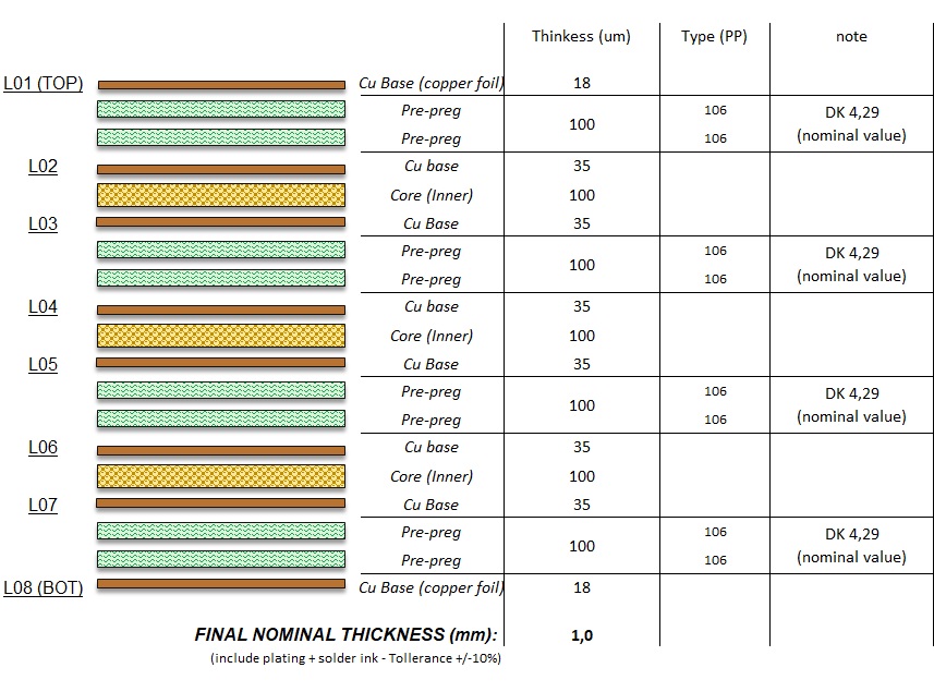
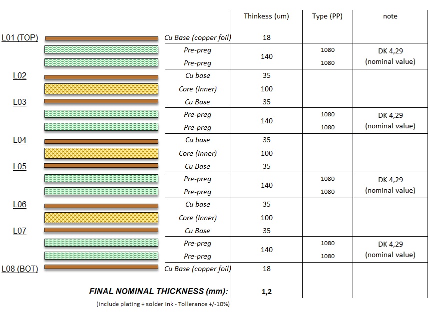
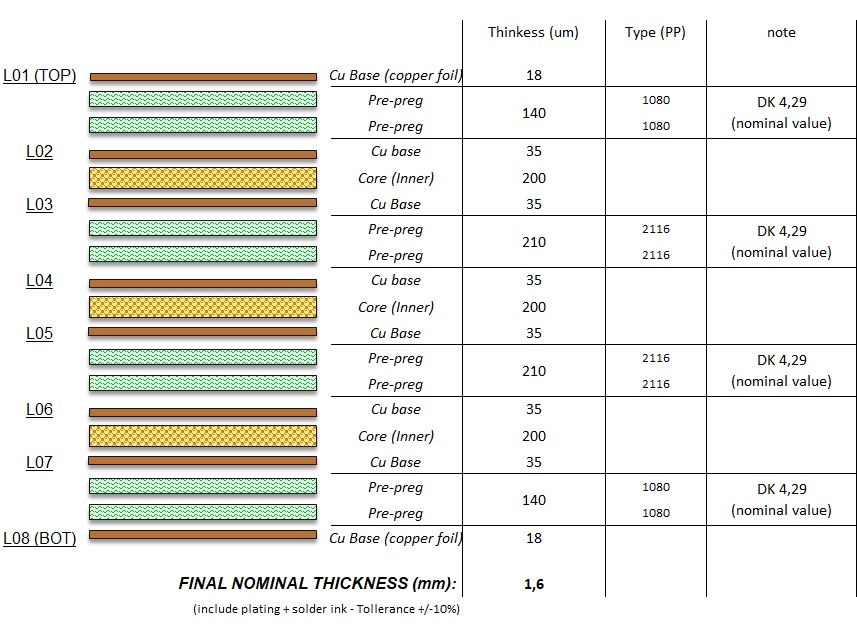
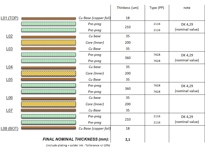
MultilayerMultilayer (Mehrschicht-Technologie):Die Multilayer-Technolo… More PCBs contain more than 2 copper layers. We differentiate between outer and inner layers, which are joined and pressed together according to a defined layer stack-up.
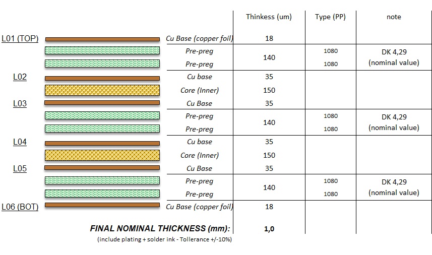
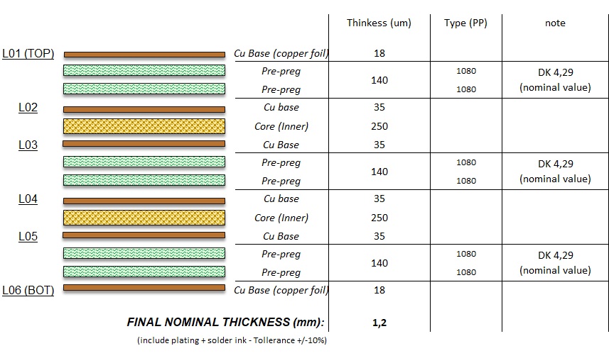
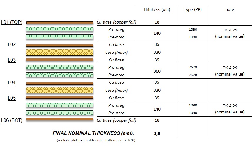
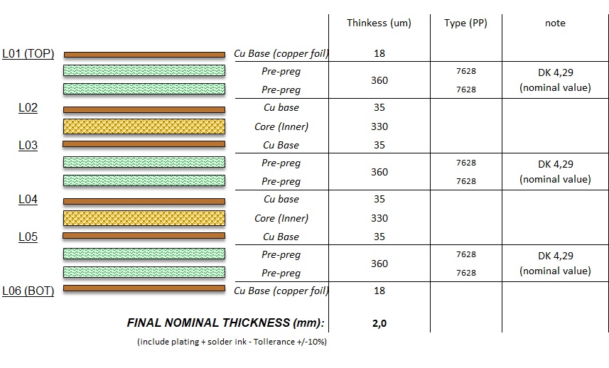
The layer stack-up basically consists of the following components:
- Copper foil
- Prepregs (glass/resin fabric)
- Material core (2 copper foils and prepregs pre-pressed to obtain a copper core)
The arrangement of the individual layers depends on the materials and prepregs available and the designer’s specifications.
Important details for the layer structure include
- Copper thickness of all layers
- Total thickness of the PCBauch: gedruckte Schaltung, engl.: PCB – Printed circuit boar… More
- Insulation distances between copper layers
(e.g. minimum requirements for controlled impedance or for electrical discharges)
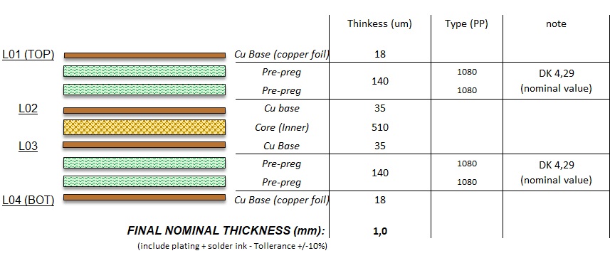
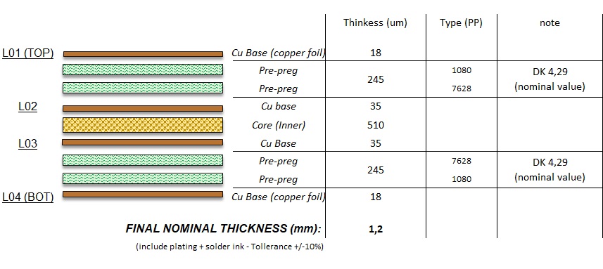
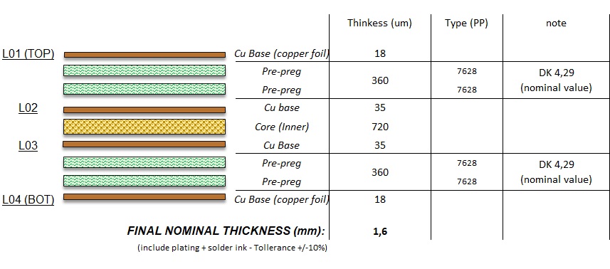
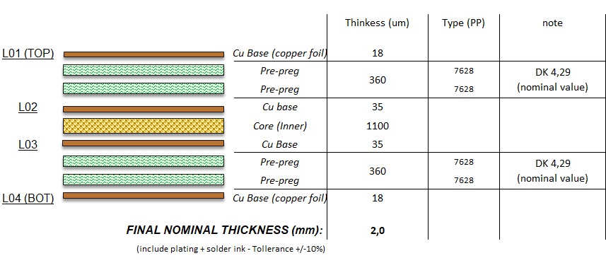
Below you will find the most common construction variants for multilayers of different thicknesses from 4-8 layers based on the available stock materials. All structures are shown with a copper coating of 18µm, but can also be realized in the same way with 35µm base copper. Higher copper thicknesses have an effect on the structure and the final thickness.
For special requirements with individual layer structures, the technical team will be happy to advise you at any time.
It should be noted that at least 2 layers of prepreg must always be used in order to achieve sufficient filling of the structures and uniform symmetry in the build-up.
- 2 layer
- 4 layer
- 6 layer
- 8 layer
Remark
These layer structures are for information purposes only and represent a standard defined in European production, which can be adapted and changed at any time.
A differentiated structure is often seen in Chinese production facilities.
For example, with a 4-layer, 1.6mm thickness, a structure with 2x prepreg 2116 over a 1.0mm core with 1/1oz copper + 2x 2116.
At 8-layers, 1.0mm, the double 106 prepreg is replaced with a 2116 prepreg.
Always discuss the layer structure with your manufacturer to avoid problems and misunderstandings.


