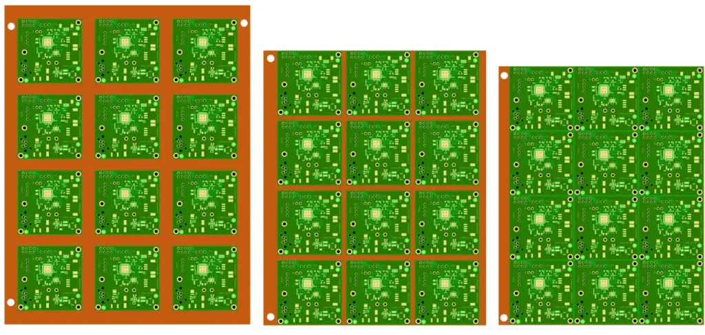
In order to supply PCBs optimally for subsequent assembly, they are preferably manufactured in a panel. Discuss the optimum panel design with your production staff or your EMS service provider. We will be happy to advise you on the optimum benefit design in terms of production and price. The benefit design is decisive for a comparable calculation between different providers. Some factors have a significant influence on the costing of your printed circuit boards.
Panel optimization

| Property | |
|---|---|
| Frame* | |
| Panel dimension | |
| Panel area | |
| Savings | |
| Costing measure | |
| Loss of utility | |
| Property | Property | Property |
|---|---|---|
| 6/6/6/6/5mm | 6/4/0/0/2,5mm | 5/0/0/0/0mm |
| 157 x 207mm | 140 x 180mm | 157 x 187,5mm |
| 3,25dm² | 2,81dm² | 2,52dm² |
| - | 16% | 29% |
| 0,27dm² | 0,23dm² | 0,21dm² |
| 35% | 16% | 5% |
| *Frame left/right/bottom/top/spacing | ||
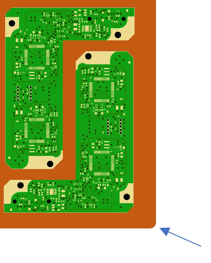
L-shaped
For PCBs with polygonal contours, e.g. L-shaped PCBs, there is definitely more scope for saving space.
As can be seen very clearly in the following example, a significant gain in space can be achieved. More PCBs can be arranged on less space.

| Property | |
|---|---|
| Panel dimension | |
| Panel area | |
| Savings | |
| Costing measure | |
| Loss/gain | |
| Standard arrangement | Interlaced |
|---|---|
| 137 x 260mm | 133 x 209mm |
| 3,56dm² | 2,78dm² |
| - | 69% |
| 0,59dm² | 0,35dm² |
| 24% | Advantage: 28% |
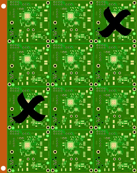
Defective parts in the panel (X-Out)
For production reasons, individual PCBs may fail in the panel during electrical testing. The average number of panels with X-outs is max. 25%. This is a generic value, depending on the purchase or production quantity, the number of individual boards in the panel and the technology used. The supply of zero defect products is only possible via sorting and requires a correspondingly higher quantity at the start of production. This is included in the calculation and therefore affects the subsequent unit price.
Packaging / sorting / marking
Panels with defective individual circuit boards are provided with a clearly visible marking of the defective circuit board, packed separately and specially labeled. On request
a marking can be applied in accordance with customer requirements. Colored marking, punching out or reflective stickers for camera machines are common.

| PCB per panel | max. X-Out |
|---|---|
| 2 to 4 | 50% |
| 5 to 7 | 40% |
| 8 to 9 | 30% |
| 10 to 16 | 25% |
| 17 to 40 | 20% |
| from 41 | max. 15% |
Number of defects per panel
The number of faulty PCBin the single panel is defined by default according to the table. If the PCBauch: gedruckte Schaltung, engl.: PCB – Printed circuit boar… More is highly complex, the failure rate can be higher and should be individually agreed between the customer and production. The focus here should be on the meaningfulness of the specifications, environmental protection and ease of assembly.
Corner rounding

It is advisable to round off the panel corners with a radius of at least 1 mm.
This serves to prevent injuries to employees and damage to the
airtight shrink foil.


