IMS / Aluminum
The ever-increasing power output of LEDs and power electronics also places ever-increasing demands on the temperature management of the PCBauch: gedruckte Schaltung, engl.: PCB – Printed circuit boar… More.
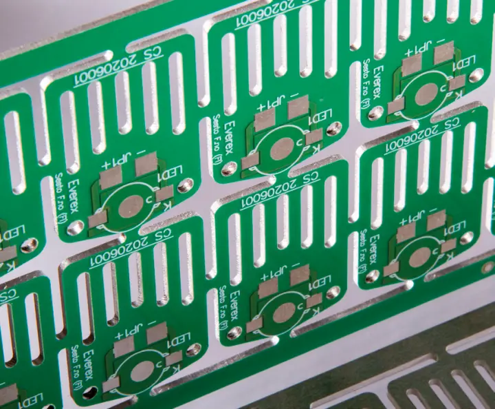
So-called IMS PCBs (Insulated Metalic Substrates) offer corresponding advantages here. The metal core is usually made of aluminum, but can also be made of pure copper.
On the one hand, the heat generated can be dissipated directly into the core of the circuit board and, if necessary, to another heat sink. On the other hand, an IMS PCBauch: gedruckte Schaltung, engl.: PCB – Printed circuit boar… More offers further advantages in terms of mechanical strength.
The advantages include
- Cost savings due to longer service life
- Platzersparnis durch verringerte Kühlmechanismen
- Power density through optimum thermal management
Compared to conventional epoxy resins, aluminum offers up to 30 times higher thermal conductivity. A further increase in the thermal conductivity coefficient can be achieved by using copper-based material. This results in an increase of up to 3 times that of aluminum.
Due to the better thermal conductivity properties compared to FR4, a higher packing density and correspondingly smaller layouts can be realised, which in turn brings further advantages.
Areas of application for this technology include high-current applications and power LEDs, Cooling of transistors, SMD and power circuit boards. The high thermal conductivity allows a quick and effective dissipation of heat. IMS printed circuit boards have been increasingly used in the automotive industry for some time now
IMS PCBs are usually manufactured as single and double-sided PCBs with through-hole vias, but are also available as multilayers.
The basic production process corresponds to that of FR4 printed circuit boards.

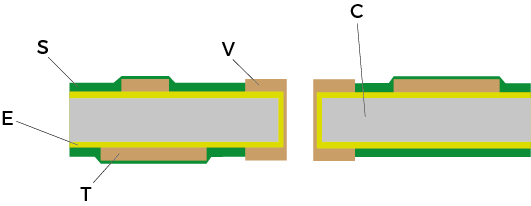
Sketched structure of an IMS circuit board
One-sided design
Double-sided design


C
T
P
S
I
V
E
Aluminum core
Track
Pad
Soldermask
Insulation
Via
Epoxy
Advantages of an IMS
- Cost savings due to higher
Service life - Space saving due to reduced
Cooling mechanisms - Power density through optimal
Thermal management
Thermal conductivity
This opens up interesting possibilities with very simple designs, to efficiently “manage” heat . The aluminum substrates are usually available in thicknesses between 0.5mm and 3,00 mm.
The copper thicknesses depend on other requirements and are available from 18μm to 105μm available. The insulation between copper and aluminum is around 100 – 150 μm ±10%.
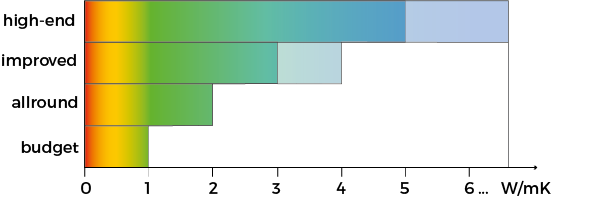
The most cost-effective variant is limited to a single-sided The most cost-effective variant is limited to a single-sided circuit with a thermal conductivity of 1.0-2.0 W/mK.
There are different qualities of thermal conductivity, starting at 1.0 W/mK up to 4.0 W/mK as standard and even up to 8.0 W/mK for special applications. For the common
applications, materials with a value of approx. 1.0-2.0 W/mK are usually sufficient.

Possible combinations
There are various possible combinations, such as multilayerMultilayer (Mehrschicht-Technologie):Die Multilayer-Technolo… More circuits with an aluminum core or a subsequently attached aluminum substrate, combined with heatsink-filled vias in a variable number of layers. However, this approach has a disadvantage: the thermal conductivity drops significantly compared to the values mentioned above. This results on the one hand from the combination with FR4 material, which has a thermal conductivity of only around 0.3 W/mK, and on the other hand from the difficulties of dissipating the heat from an internal aluminum core.
The variant with the aluminum attached to the outside offers the advantage that the finished circuit can be pressed onto the aluminum using special thermally conductive prepregs. These prepregs have almost identical thermal conductivity properties to the aluminum substrate (also 2.0 W/mK), which means that the restrictions are minimal. This gives the layout designer considerably more scope for design.
Vias filled with heatsink paste provide a thermally acceptable heat transfer to the aluminum. This technology enables the most effective dissipation of heat, especially in more complex circuits where this is essential.
Design rules
Due to the pressing on of the copper foil and the almost constant chemical processes for creating the conductor pattern, there are no restrictions on conductor track widths and spacing.
The following criteria must be observed for drilling processes:
In order to ensure perfect drilling without contacting the aluminum core, it is necessary to pre-drill the aluminum carrier with larger holes. This makes it possible to use epoxy resin or plugging paste to keep the subsequent hole separate from the aluminum carrier. This principle also makes through-hole plating possible.
Attention: larger drilling add than for standard PCBs!
A plated-through hole through the aluminum carrier with a final diameter of 1.0mm is generally drilled in PCBauch: gedruckte Schaltung, engl.: PCB – Printed circuit boar… More production with an add of 0.15mm, i.e. 1.15mm. This achieves the desired final diameter of 1.00 mm after the copper has been built up in the hole. If additional pressing with aluminum is required, the hole should be drilled a further 0.45 mm larger (1.00+0.15+0.45=1.6 mm).
The challenge arises when the hole positions in this scenario are about 1.6 mm apart. At first glance, there appears to be sufficient space for residual rings and spacers. However, there are overlaps in the aluminum carrier, so that no aluminum remains between the drill holes, only epoxy resin or plugging paste. This has only a minor effect on heat dissipation, which mainly occurs via the sides of the beam, with few overlaps. However, with a large number of such overlaps, entire areas of the aluminum carrier could be filled mainly with less thermally conductive resins. In extreme cases, this could impair the stability of the aluminum beam, and in production there is the general problem of drill breakage due to overlapping drill holes.
As a rule of thumb for the arrangement of holes in relation to each other, the following can be taken into account for safety reasons
Distance between two drilling centers = r1 + r2 + 0.7 [mm]
General characteristics
| Characteristic | Value/content |
|---|---|
| Material | Aluminum | Epoxy resin-Fibreglass |
| RoHS | Yes |
| UL certified | Yes, UL 94V-0 |
| Standard tolerance | ±10% |
| PCB thickness | 0,5-3,0mm |
| Min drill | 0,8mm |
| Dielectric constant εR | 3,8 (at MHz) |
| Loss factor | ≤0,03 |
| Dielectric strength | >40kV/mm |
| Surface resistance | 5,0Ω*10e15 |
| tracking resistance CTI | >175 |


