Warp & Twist
Consistent layer design
A homogeneous or symmetrical copper balance within a PCBauch: gedruckte Schaltung, engl.: PCB – Printed circuit boar… More is important to prevent twisting or warping. Irregular copper distribution can lead to material stresses in the PCBauch: gedruckte Schaltung, engl.: PCB – Printed circuit boar… More and to problems during assembly or subsequent mounting! The twisting and warping according to IPC-A-600 / IPC-TM-650 must not exceed 0.75% for SMD PCBs or 1.0% for pure THT PCBs!
Further influences of asymmetrical copper distribution
In reality, a balanced design has a fairly strong influence on galvanic distribution, such as:
Final copper thickness distribution
Different copper thicknesses on the PCBauch: gedruckte Schaltung, engl.: PCB – Printed circuit boar… More surface at different positions
Result of copper etching
This can result in a non-uniformity of the copper pattern (conductor widths and gaps between the conductors)
Irregularities in the solder resist
Uniformity of the thickness of the solder mask across the PCBauch: gedruckte Schaltung, engl.: PCB – Printed circuit boar… More surfaces (due to differences in copper thickness after coating the PCBauch: gedruckte Schaltung, engl.: PCB – Printed circuit boar… More surface)
|
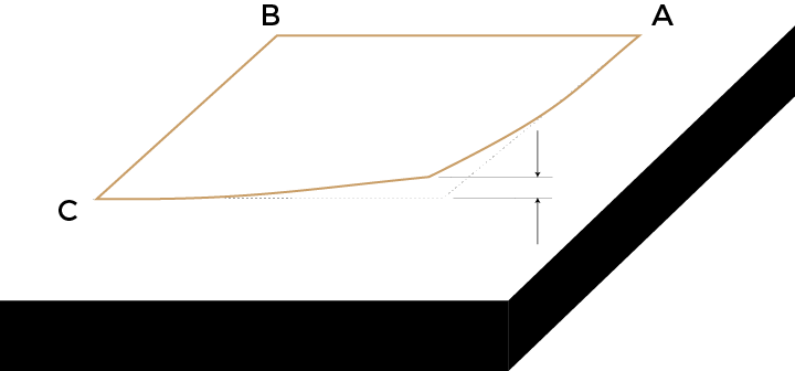
Warp (Bow) |
Twist (Twist) |
|---|---|
| Curvature of the circuit board when all 4 board corners are on the same level. | Deformation of the PCB. There are at least one corner is not on the same level as the remaining board corners. |
| Bow = max. height / length * 100 | Twist = max. height / 2x diagonal * 100 |

All 4 corners rest on the tabletop. The circuit board bulges in the centre.

3 corners rest on the tabletop. One corner bulges out.
Causes for Bow & Twist
The main causes of twisting and warping lie in the asymmetry. On the one hand, the symmetrical layer structure plays an important role. However, symmetrical copper distribution is also very important.
If it is not possible to achieve complete symmetry for design or development reasons, discuss the layer structure directly with the manufacturer you trust.
- unbalanced copper distribution
- avoid full-surface areas
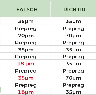
- avoid asymmetrical layer build-up
- uniform copper thicknesses from the outside to the inside
- even copper distribution on the reference layers
- even spacing from the centre to the outside
- Mechanical and thermal stress influences
during production - different coefficients for material expansion
- unbalanced blind and buried vias
- press-fit plug (avoid stress when pressing in)
- improper storage
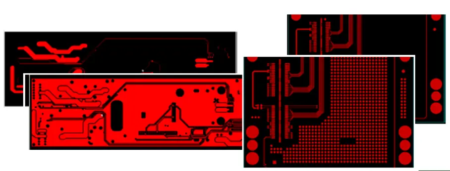
unbalanced copper distribution
equalisation of copper symmetry via areas
(gridded or dotted also possible)

asymmetrical layer stackup


